
 Jean-Marie Brunet | Senior Director of Marketing, Product Management and Product Engineering | Siemens EDA
A Systematic Approach to Verification and Validation Using Hardware-Assisted Verification
Success in the semiconductor industry today is defined by software performance. Meeting hardware (IC) specs is now only one of four mandatory criteria to meet the success metrics. Achieving performance and power targets; processing workloads, frameworks and benchmarks; and verifying system-on-chip (SoC) functionality within the overall system context are the others.
Achieving success means that the complex SoC structure needs thorough verification at every stage of the design and verification process at a reasonable cost-per-verification cycle. This demanding scenario is dramatically changing the chip design verification and validation landscape, promoting the hardware-assisted verification platform to an essential role in any verification strategy.
A comprehensive hardware-assisted verification platform must offer a powerful verification environment to manage the more difficult SoC designs, including AI/ML, 5G, and automotive. By linking hardware emulation and FPGA prototyping, and adding a complete software test environment, verification groups can tackle design complexity that resembles a multi-layered Lego-like structure, tougher requirements for low-power consumption and high-performance and software content.
The importance of verification cannot be overstated. It consumes 50% of the project design cycle, a result of a number of factors, such as single- and multi-die design complexity, computing power, I/O traffic activity, energy consumption and the use of many more peripherals than were used in previous generations of designs. Verification impacts quality, cost, and schedule because it prevents designs from failing at first silicon. A re-spin of a large design taped out at a node below 10 nanometers could cost more than $10 million. A product delivery delay of several months could cost hundreds of millions of dollars.
Market Trends Bring Change
While change to the verification flow is inevitable due to performance and complexity, several market trends in chip verification and validation intensify the need and drive the move for better integrated hardware-assisted verification tools.
Vertical market segments have more demanding needs and often serve as leading indicators that propel trends. Four major markets –– networking, communication including 5G, computing and storage, automotive and other forms of transportation –– share the same challenges when designing, verifying, and realizing a chip. Meeting power consumption and performance targets is one facing all of them, as is the software content of their SoC designs. Their chips now consist of a combination of hardware and software with software becoming the dominant contributor. The hardware/software combination pushes verification costs higher than design costs, especially software validation expenditures.
Software performance is the most significant trend today. An SoC design software environment requires massive amounts of cycles to run. Billions of cycles are needed for booting operating systems, running benchmarks and applications. A long list of different workloads or benchmarks must be executed to certify a design in any vertical market. Artificial intelligence, machine learning and deep learning designs run different types of frameworks or workloads. The same is true for advanced driver-assisted systems (ADAS) where loads of sensor and raw sensor fusion data must be processed. For the mobile market, AnTuTu is the main reference. Graphics designers run Kishonti-type benchmarks.
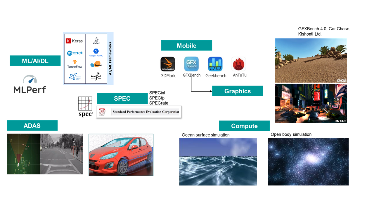 An SoC design software environment needs billions of cycles for booting operating systems, running benchmarks and applications with different workloads or benchmarks to certify a design in a vertical market. Source: Siemens EDA
Streamlining a Complicated Verification and Validation Landscape
Chip design verification groups need an effective verification and validation solution to approach verification using the right tool for the right task. Equally, tool suppliers need to approach verification and validation within the context of the right tool for the right task, an approach that hasn’t always been provided. The answer is a comprehensive hardware-assisted verification system comprised of hardware, software and system verification that streamlines and optimizes verification cycles while helping reduce verification costs.
Hardware-assisted verification is defined as special purpose hardware to accelerate verification, typically hardware emulation and field programmable gate array (FPGA) prototyping, both desktop and enterprise FPGA prototyping engines, to handle the size and complexity of SoC designs. It should add virtual platforms to validate software as well. A platform like this includes design visibility, accurate analysis and comprehensive debug tools to estimate and measure power and performance while processing massive workloads so that throughout the verification cycle different milestones can be met each with a different need.
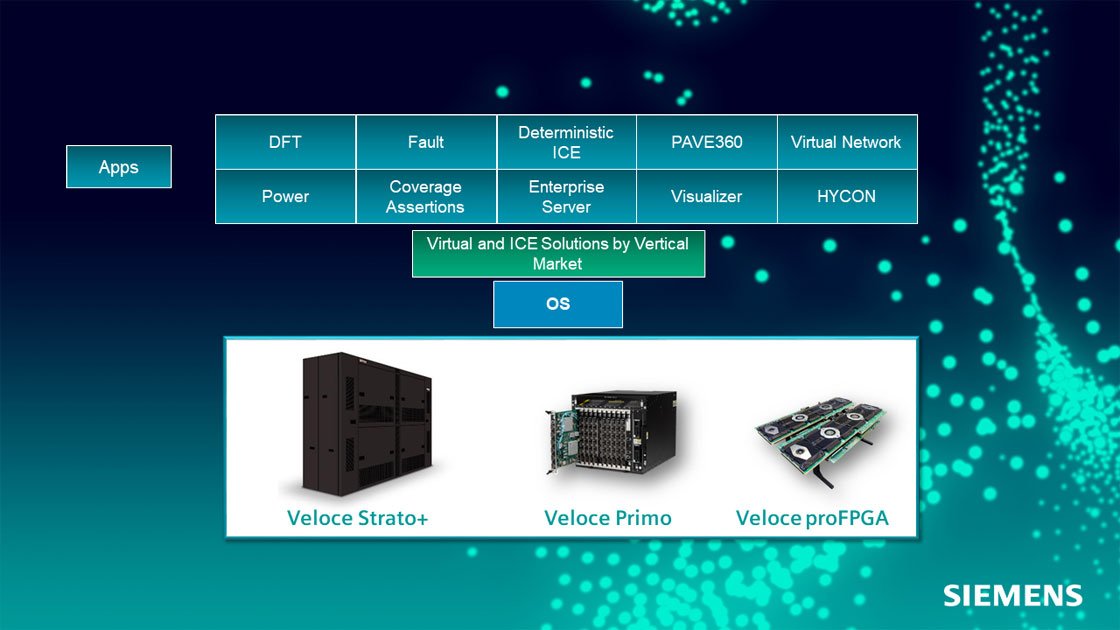
Hardware-assisted verification includes hardware emulation, desktop and enterprise FPGA prototyping and a software test environment. Source: Siemens EDA
Deploying a hardware-assisted verification platform is a systematic approach, taking into account the various steps for complete and thorough verification. Early on, the complete design is not available yet and the work is at the architectural level. Therefore, the virtual platform with virtual models is used to process software workloads. Tight integration between the virtual platform and the emulator enables the emulator to take charge of RTL design blocks.
Once RTL code becomes stable, it needs to be debugged with full design visibility. Different verification use models are required along with scalable design capacity. These tasks need an emulator able to perform power analysis and gate-level emulation. The gate-level netlist is available closer to tape-out and that needs accurate power analysis done with the emulator.
A new concept called “emulation offload” offloads emulation tasks to enterprise FPGA prototyping tools. Early in the verification flow, an emulator is needed to provide accurate and efficient RTL debug. Once the design becomes more stable and less buggy, it needs to be verified at a higher speed. At this stage, debug is traded for speed and accomplished by offloading the design from the emulator to the enterprise prototyping tool to accelerate the verification cycle and reduce the cost of verification task.
The final piece to complete the platform is a desktop FPGA prototyping, a single-user, smaller footprint type of prototyping tool that sits on the desk or in the lab for easy bring up and very fast execution.
The ROI of Hardware-Assisted Verification
While a hardware emulator is the most expensive of the tools making up a hardware-assisted verification platform, its total cost of ownership has dropped considerably over recent years.
A hardware-assisted verification platform is a cost-effective verification solution when measured on its verification power and flexibility. As a versatile verification platform, it has the performance and capacity to handle the most complicated debugging scenarios that often include embedded software content.
The acquisition cost is amortized through a multi-user support model and offers an attractive return on investment (ROI). A team of application engineers on hand to operate and maintain a hardware emulator is no longer needed, and it can now be used in virtual mode with no manual intervention. Improved reliability further reduces the cost of maintenance.
Conclusion
Hardware-assisted verification is a systematic approach to chip design verification and the only option when hardware and software meet. By combining emulation, FPGA prototyping and a virtual platform to work on the same SoC design, chip design verification groups can assemble a complete hardware-assisted verification system for thorough and exhaustive verification and validation. Its strategic value makes it destined to be the foundation tools in all chip design verification flows.
___________________________________________
About Jean-Marie Brunet
Jean-Marie Brunet is the senior director of product management and engineering for the Scalable Verification Solutions Division at Siemens EDA. He has served for over 20 years in application engineering, marketing, and management roles in the EDA industry, and has held IC design and design management positions at STMicroelectronics, Cadence, and Micron, among other companies. Jean-Marie holds a Master of Science Degree in Electrical Engineering from I.S.E.N Electronic Engineering School in Lille, France. Jean-Marie Brunet can be reached at jm_brunet@mentor.com.