
 Scott White | CEO | PragmatIC Semiconductor
Scott White, CEO at PragmatIC Semiconductor, has often been referred to as a serial entrepreneur. Not surprising really since in addition to PragmatIC, a pioneering flexible electronics company headquartered in Cambridge, UK, he has built and sold five other technology businesses, living and working across the globe. In this interview Scott outlines some of the challenges and opportunities he sees for the semiconductor industry.
Tell us a bit about your background. It sounds like you have travelled around quite a bit!
Yes – I grew up in Australia, but I have been lucky enough to also live in Asia, the US and the UK. My university degree was in mathematics and information technology, with a thesis on neural networks and machine learning – long before the recent explosion in interest around these techniques. However, over the past 25 years my career has been focused on business management and technology commercialisation.
What is PragmatIC doing differently? What was your business concept?
We produce silicon-free flexible integrated circuits (ICs) that are thinner than a human hair and 10x lower cost than traditional silicon chips, creating the opportunity for intelligence in everyday objects. Our core concept was a unique “fab-in-a-box” for semiconductor manufacturing – we call it FlexLogIC – that enables local just-in-time production with 100x lower capex than conventional fabs. Although we sell our own ConnectIC family of ICs for radio frequency identification (RFID), our primary business model is as a foundry. The breadth of applications being addressed by our customers is astounding, but I am most excited by the increasing focus on solutions for key UN sustainable development goals such as circular economy, food waste and ubiquitous healthcare.
What hurdles did you face in developing your tech?
I think the most significant challenge by far was our core technology development to deliver a reliable and scalable manufacturing process for non-silicon ICs. We demonstrated a basic proof-of-concept thin film transistor on a plastic substrate very early on. But extending this to incorporate everything needed for an integrated circuit (including resistors, multi-layer conductive interconnects, vias, contact pads, etc) required a series of engineering innovations, particularly when constrained by our critical objectives of low cost and mechanical flexibility. And, of course, transferring that process to industry-proven fabrication tools (within those same constraints of cost and flexibility) posed additional challenges – all ultimately overcome by our “pragmatic” approach of blending conventional semiconductor manufacturing experience with novel materials and processes, and evaluating the key trade-offs without bias or preconceptions.
What do you see as the biggest issues for the semiconductor industry now?
Three main topics have become prominent recently: chronic supply/demand imbalance; concentration of supply chains and resulting geopolitical concerns; and the carbon footprint of electronics manufacture. However, these issues have actually been present in the industry for decades (if not quite so extreme as today) and result from key structural challenges in semiconductor manufacturing, arising from increasingly complicated and energy-intensive fabrication processes, and leading to increasingly high R&D costs and even higher fab capital expense.
While I don’t see an easy solution to these problems for high-end applications (such as automotive and AI) that are pushing the boundaries of silicon functionality every year, there is an opportunity to avoid them for other markets. A good example is the rapidly expanding Internet of Things, where approaches such as PragmatIC’s can deliver suitable functionality at a far lower cost than conventional silicon, while also supporting highly localised manufacturing models and dramatically reducing the environmental impact of semiconductor fabrication.
Surely, we already have chips with everything, where is the market for yours?
Well actually, there is huge potential in so many different market segments, so it’s hard to give just one answer! However, the opportunities I am most interested in are those that aren’t just more sophisticated electronic devices, but rather adding novel functionality and interactivity to things that we would not normally associate with electronics.
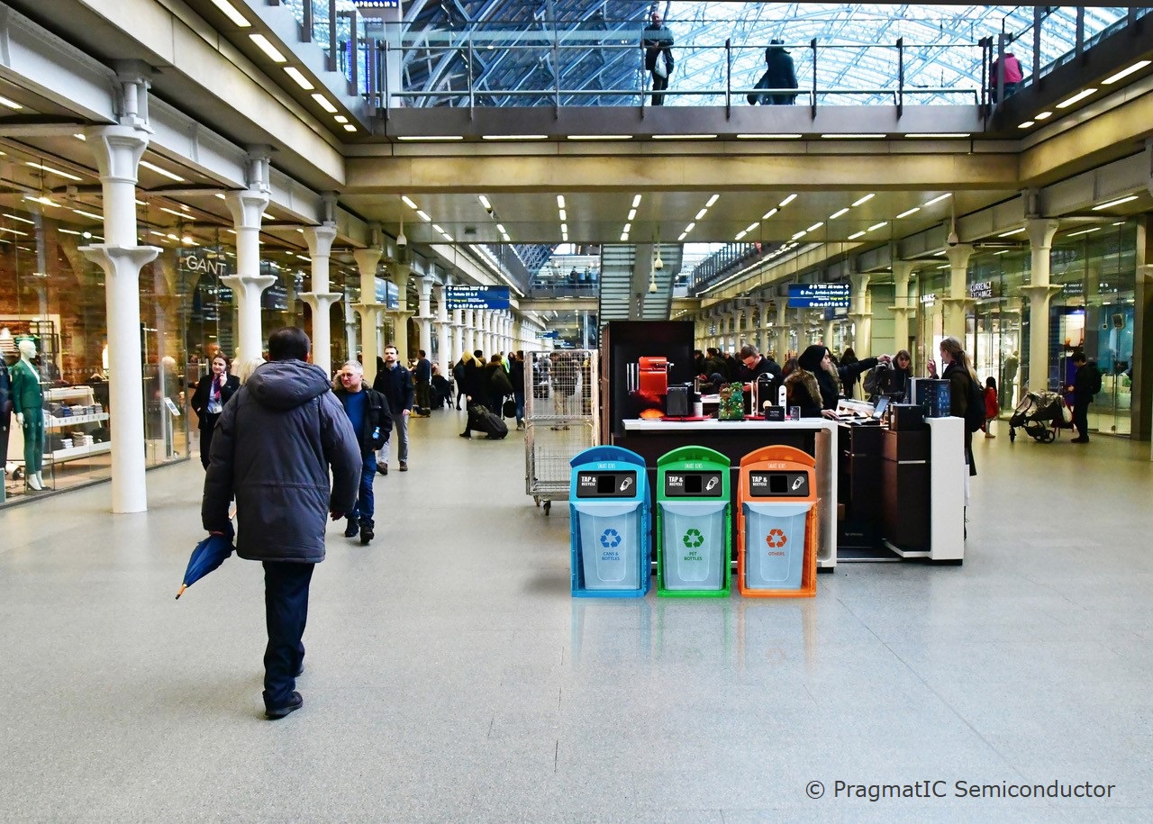
Radio frequency identification (RFID) is a great example of this, where wirelessly readable unique IDs are now used on billions of consumer goods to dramatically improve inventory control (particularly for retail apparel). With PragmatIC’s technology, RFID can be extended to a wider range of products and use cases. For example, we have customers focused on increasing the reuse and recycling of plastic drinks bottles and other similar packaging; authenticating and tracking pharmaceutical products for safety and patient compliance; and automating traceability and improving the efficiency of pathology testing.
Adding sensing and some modest compute power opens up even more exciting opportunities. Imagine being able to monitor food freshness at every step of its journey from farm to fork, improving the quality of food reaching consumers while also eliminating unnecessary waste in the supply chain. Or transforming a regular wound dressing into a smart bandage that can monitor healing without disturbing the wound or requiring dedicated time from a medical professional.
More broadly, the semiconductor industry has massive opportunities to address key global challenges, such as the sustainable development goals set out by the UN. From PragmatIC’s perspective, we have seen the majority of our recent customer business focused around three key themes: circular economy, sustainable agriculture, and ubiquitous healthcare.
Can you give us your vision for the semiconductor landscape in 5, 10 or 20 years?
I think the semiconductor industry is too diverse to have a “one size fits all”, but I have a clear vision for what our segment of it could look like: hundreds of modular fabs providing distributed production of flexible ICs around the world, mostly on-site at customer premises. These are managed via a fab-as-a-service model, giving customers the benefit of closely integrated and strategically controlled electronics supply, without them needing to become experts at semiconductor manufacturing. Production cycle times of less than 24 hours mean that product mix can be adjusted daily in response to market demand, and new flexible ASIC hardware can be introduced as rapidly as we currently develop software. The minimal energy requirement of these fabs, also leveraging cogeneration for improved efficiency, can be entirely met by sustainable sources. And the resulting trillions of flexible ICs are used to release the immense potential of intelligence in everyday objects, in ways that enrich our life by reducing complexity rather than adding it!