Paper Submitted by Ross Miller, Vice President of Strategic Marketing & Business Unit, SkyWater Technology and Mohamed Kassem, CTO & Co-Founder, Efabless
Wow, 2020 has been a year, hasn’t it? It is going to be remembered for lots of things, including this unprecedented pandemic. Although many industries have been negatively impacted, innovation continues. And, for a very select group, the list of things to remember will include a pivotal milestone for open source application specific integrated circuit (ASIC) design. In June of 2020, Google and SkyWater Technology collaborated to release the industry’s first open source foundry process design kit (PDK) known as SKY130 (130 nm CMOS technology) under an Apache 2.0 license, giving designers worldwide access to use the technology for new IP functions as well as complete open source ASICs.
Some people think the open PDK achievement is brilliant, some say crazy, for others it was just a matter of time. Regardless of your opinion, fully open ASIC design is here in a great experiment that is happening right now. In this article we will summarize several points to get you up to speed.
You may think of the 130 nm process as a lagging or legacy CMOS node, but we believe it is a workhorse for mixed-signal applications that are heavily used in IoT applications for things like edge computing, power management, smart sensor integration and a myriad of variations on those themes. We also believe that with specialized component integration and design innovation, customers and designers will extract more value from such a versatile and cost-efficient “legacy” process. It is also worth mentioning for some historical context that Intel’s 2GHz Pentium 4 processor was developed using 130 nm technology – an example of custom design innovation.
For the referenced IoT category applications, 130 nm technology offers an ideal value point for analog-heavy applications that also require digital logic. This experiment of opening IP development on this widely used node is ideal in that it has a very large pool of existing IP given its maturity, and from a technology perspective is well-positioned to address the needs of the rapidly growing IoT segment. These dynamics, along with a significant focus in the industry on “More than Moore” concepts, combine in a very relevant way at a time when there is increasing pressure to accelerate time to market, reduce costs, and increase data and IP security.
This has placed emphasis on gaining maximum performance out of mature process technologies by customizing them for various applications. Beyond that, pushing performance requires optimizing design IP to improve circuit performance of ASICs (e.g., improved speed, lower power, higher density). As this thrust in the industry matures, the voices of those advocating that open source concepts can accelerate these pursuits are growing louder.
Open Collaboration Supports IP Performance Optimization
Looking back several decades at the evolution of the semiconductor industry, we see a trend of focusing the most human capital on IP development for leading edge technologies. This has led to the pursuit of producing IP for the highest value ICs and riding Moore’s Law of transistor scaling to drive the most IC performance gains. This dynamic combined with the predominantly closed nature of chip design has led some to believe that a trail of unoptimized IP has been left in the wake of transistor scaling. Some proponents of open source IC design advocate that opening IP development to a wider pool of talent can not only optimize development, but in an open environment, contributors can reuse IP produced by others rather than beginning from scratch. Designers can then improve it and make it available for others to do the same in a subsequent iteration. This can be especially valuable for legacy nodes which remain heavily used for IoT and mid-market consumer and industrial products.
The open source model offers a stark contrast to the traditional closed source model where proprietary IP produced by for-profit companies take solutions as far as their talent is capable or to the point that meets their identified needs. Unfortunately, years later a product developer in a different industry or at a different company working to solve the same or similar problems will likely not have access to past work they could leverage to make next-generation products perform even better.
Transparent Architectures Can Improve Security
In addition to the prospect of improving IP performance on a large scale for legacy technology nodes, open source concepts are touted as an ideal path for enhancing data security. On the surface, this may sound counterintuitive. How can chips designed with open IP offer data security that’s worth anything? It’s a good question. The way to think of this is to recognize when a vulnerability is found with closed source software, it may not be brought to the attention of the IP owner or the person whose data is passing through the device. Conversely, security architecture based on open source concepts can be freely scrutinized by a world of IP developers. Vulnerabilities are more likely to be openly identified and thus remedied by stakeholders. Over the long term, the collective contributions to enhance performance of these security aspects can build up a more robust ecosystem. This concept is being pursued for the OpenTitan root of trust initiative supported by Google (and several other leading technology companies), which is currently developing as an alternative to closed source proprietary security architectures.
What has changed in the industry for me to care about open source IC design?
A Completely Open ASIC Value Chain
The concept of open source design in the semiconductor industry isn’t new, but all the components to make this process fully manufacturable haven’t been available together until now. Thanks to recent developments in the market there is now a fully manufacturable open source PDK and related resources for 130 nm mixed-signal CMOS technologies as illustrated in figure 1.
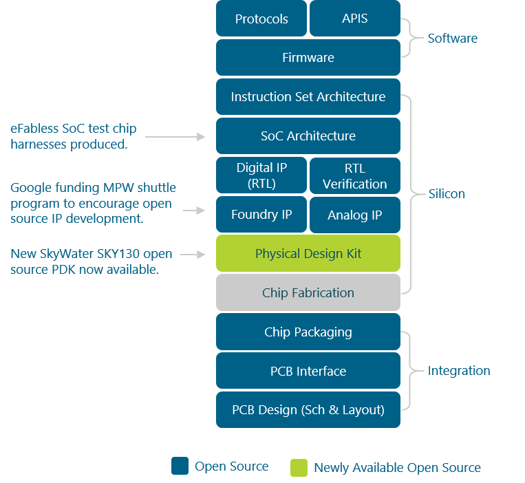
Figure 1: The release of the SKY130 PDK completes the open source value chain for 130 nm custom ASICs.
Open EDA Tools Have Quietly Evolved
In addition to the completion of the open source value chain, open source EDA tools have matured steadily over several decades. Today, a number of environments are used with the open PDK: Magic VLSI, Klayout, Yosys, Netgen, OpenROAD and openLane. While a significant distinction exists between capabilities and services of these platforms vs. conventional industrial EDA tools, there is noteworthy progress as a growing number of users and developers around the world are continuously driving their evolution.
Is end-to-end open source chip design even realistic for commercial applications?
What’s the future for open source ASICs? It’s obviously difficult to predict. While the potential behind open source design is exciting, the conventional closed IP model and traditional EDA development process will continue to play a dominant role in the industry, delivering the high level of service that a large segment of the market needs and expects. However, we also expect the developing open source ASIC value chain to drive more adoption of these concepts.
To support this pursuit, Efabless has developed open source SoC test chip harnesses that will be available for IP developers to use on the SKY130 process and will support broader engagement of the open source community for IP development. This will reduce yet another barrier for engagement and enable developers to focus on specific aspects of IP performance and test them on a functioning chip.
One of the age-old arguments against open source concepts is: How can you generate revenue, much less profit, if you are giving away your IP for free? The problem here is the underlying assumption that open source (ASIC design in this case) is free. If it has a future life in commercial business, it will not be free. It will blow past the traditional royalty-based model and incorporate IP as a service model.
When framed in this way, it’s not all that crazy. We’ve seen service-based transaction models spring up across all parts of the economy with wild success. The Linux/Red Hat story is one we repeatedly refer to as a very relevant example of high value open source software that is delivered to users as a service that generates significant revenue. A testament to the value of this model in this case is the acquisition of Red Hat by IBM for $34 billion in 2019 to enable future hybrid cloud services.
Open Source Outlook and Areas of Need/Opportunity
While open source activities may not be getting the biggest headlines, there’s a lot happening that’s building a foundation for change. DARPA support of open source chip design is notable through the IDEA program. In 2017, the CHIPS Alliance was founded and currently has 25 members organized around a charter to accelerate the open hardware ecosystem. Perhaps among the most well-known successes of open concepts in the semiconductor space is the RISC-V open instruction set architecture that was introduced in 2010. In addition, Google’s longtime advocacy of open support concepts and recent leadership within the ASIC domain has led to a surge of interest that is spilling over into the semiconductor industry.
Looking ahead for the open source ASIC story, there are several areas that will require action to move the initiative forward and increase adoption. The first area is further maturation of the IP support services model. This is critical because in order for IP that is produced by the open source community to be broadly useful, it needs to be standardized and documented in a reasonable fashion. While this can be something that develops organically, we know from looking at the Linux/Red Hat model that proactive stewardship can drive adoption and bring order to streamline product experience for users. Today, Efabless is building a digital portal to address this exact need for support services with the goal of enabling users to harness the value of open source IP along with the speed and reliability needed to produce industrial grade ASICs.
An open source offering holds promise for accelerating innovation by removing barriers and obstacles relating to experimentation and collaboration for IC design. The traditional model of proprietary development is now augmented with a new approach inspired by open source software and based on rapid trial and error with a global community of designers who collaborate, design and verify. This is the true value behind open source PDKs. By working together, sharing knowledge and building on others’ improvements, our industry is on the path to improving value by combining open and “More than Moore” concepts.
More Information and Resources
Below are additional resources to learn more about this rapidly developing area of open innovation.
- The FOSSi Foundation has an active speaker series on the topic of open source ASIC design using the SKY130 PDK.
- A number of technical papers authored by Google and Efabless were presented at ICCAD 2020 (Nov 2 – 5, 2020). The conference also included a Workshop on Open-Source EDA Technology (WOSET).
Following is information on how to access the open source foundry PDK and the Google-sponsored MPW shuttles:
- The open source foundry PDK (SKY130) is accessible now at https://github.com/google/skywater-pdk.
- To stimulate use and adoption of the SKY130 process, Google has sponsored a series of six MPW shuttles each with 40 design seats and is accepting designs from any individual, company or academic group to ride on the shuttles and receive silicon with zero cost to the designers.
- Efabless is supporting the initiative to ingest and aggregate designs for the series of sponsored shuttles.
Interested parties can learn more about SkyWater’s PDK open source foundry offering by visiting https://skywater-pdk.slack.com/ and/or by contacting: swfoundry@skywatertechnology.com.
_________________________________________________________________
About the Authors

Ross Miller
Ross Miller has over 15 years of experience in process engineering, technology development, project management, and sales and marketing leadership. At SkyWater, he leads the marketing and communications team and the business unit which manages go-to-market activities for the company’s technology platforms. Ross received a B.S. in Physics from the United States Air Force Academy and an M.S. degree in Electrical Engineering from North Dakota State University.
 Mohamed Kassem
Prior to launching efabless.com, the first semiconductor company applying open community innovation to all aspects of product development, Mohamed held several technical leadership and management positions with Texas Instrument’s Wireless Business Unit. Notably, he was responsible for integrated analog IP design from 180nm through 28nm from technology inception to qualified volume production for TI’s mobile phone applications processors OMAP. Mohamed received an M.Sc. in Electrical Engineering from the University of Waterloo.