
Paper Submitted by Dave Kelf, Vice President of Marketing and Chief Marketing Officer, Breker Verification Systems
The advent of cloud computing has opened new opportunities for extensive data processing. Coupling cloud-based Internet of Things (IoT) solutions with Artificial Intelligence (AI) has enabled a panoply of application opportunities. Highway control, winery growth patterns, automated surveillance all represent diverse examples.
The use of AI semiconductors that can apply Machine Learning (ML) to accelerate these applications is key. Be they part of the cloud infrastructure, or operating on the IoT edge, AI provides automated analysis never before possible. AI companies and projects have sprung up, producing ingenious architectures for ML devices. Verifying these devices requires different thinking, given their dynamic operational capability and sheer size.
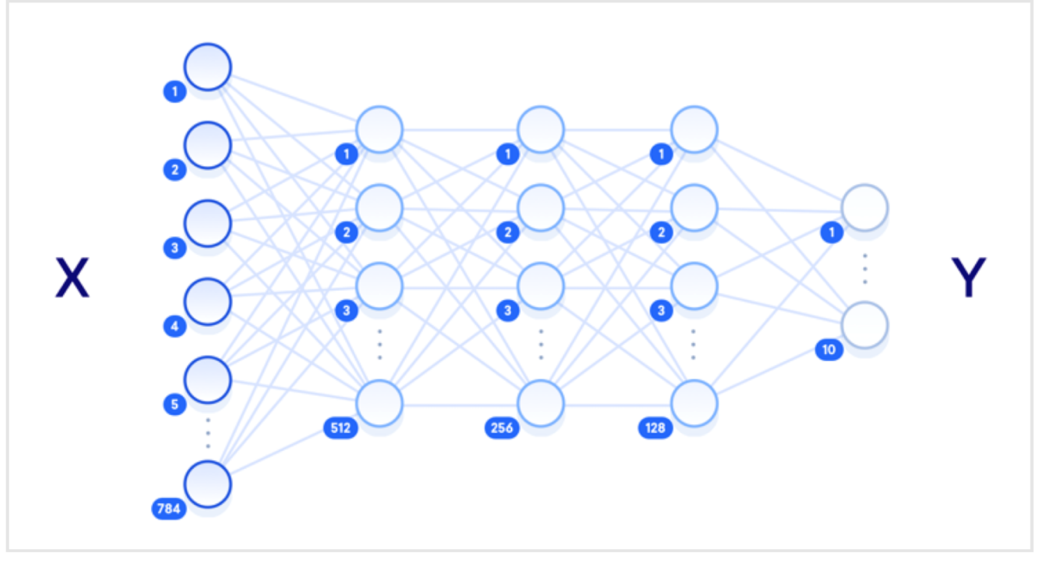
Figure 1 caption: A Convolutional Neural Network consists of a fully interconnected processing nodes. (Courtesy: Ellie Birbeck, DigitalOcean)
Modern Machine Learning is based on the idea of a system that can read a large amount of data on a specific subject to produce a model. This model then enables the recognition of new information on the same subject. The implementation of these solutions is usually performed using a Convolutional Neural Network (CNN), see figure 1.
A CNN consists of a large number of processing nodes that are fully interconnected, much like the neural network in a human brain. Each processing node usually performs multiply accumulate functions, such as those found in many digital signal processing convolution algorithms. Coefficients are provided to each processing node to weight its effect. The number of node layers (hidden layers) between the input and output nodes depicts the depth of the CNN. A large number of hidden layers suggests greater depth to the learning algorithm and is therefore termed Deep Learning.
Let us use the example of a handwritten number recognition system to illustrate how this works. Figure 2 shows a CNN being fed with handwritten numbers, which may be input as a pixel map of 256 pixels for each number. The pixels are then fed to the 256 input nodes as a grey scale number. The input nodes multiply these pixels by coefficients before then passing the result to the next layer, which successively performs the same operation until the result reaches the final layer. This final 10-node layer is set up so one of the nodes will output a 1 against the specific number input.
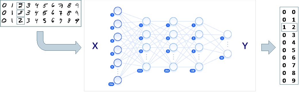
Figure 2 caption: A Digit Recognition System may use up to 256 pixels for each number on a pixel map. Courtesy: Ellie Birbeck, DigitalOcean)
Now, by setting up the right coefficients, it is possible to recognize these numbers to a level of accuracy close to 100%. To set the coefficients, a large amount of data is provided together with the correct outputs. Algorithms are applied to change the coefficients to get the output to home in on the right result. Ultimately, this matrix of coefficients, or model, may then be applied to the same neural network. When a new handwritten number is input, it will be recognized by the system.
This same approach may be used to provide image matching, audio recognition, and even pattern analysis. For example, imagine continuously collecting a large amount of data from IoT temperature and humidity sensors attached to grapevines in a winery. This could allow a system to predict which grapes across a hillside will produce better wine by learning and then analyzing historical patterns, as shown in figure 3. Data from the sensors is passed to the cloud where it is stored and analyzed by an ML system to provide a model. From then on, as new data is directly fed to the cloud-based ML system, it provides predictions as to the quality of the grapes on different parts of the field, and can even make suggestions as to different watering regimes, fertilizer, etc.
As with all semiconductor development, functional design verification is often the critical path and it is no different with these devices. ML designs pose a new issue: the functionality of these chips evolving as the device learns. Trying to come up with a set of test vectors with checks that operate across the entire system with its evolving coefficients and network is extremely complex. Tracking down corner-cases in a system where a small error in one evolving node can result in large issues many nodes and several timing cycles away, presents a huge debug challenge. Producing a coverage metric that captures diverging coefficients equates to guesswork.
Given the regular array structure of the CNN, it could be argued that it is sufficient to verify just one node exhaustively, and then rely on a high-level validation of the architecture of the overall system. However, the devil is very much in the details in these chips. For example, many of them operate using floating-point numbers that can scale up very quickly if an error occurs.
The verification of these, and many other complex scenarios, can be greatly improved if test content generation can be performed using some AI solutions of their own. For example, one powerful algorithm used in ML to refine the coefficients is backward propagation. Backward propagation works by starting with the known output and working backwards through the neural network to predict the optimal coefficients.
A similar idea can be applied in verification using AI Planning Algorithms. IBM’s Watson team defines a Planning Algorithm as:
Planning is a long-standing sub-area of Artificial Intelligence (AI). Planning is the task of finding a procedural course of action for a declaratively described system to reach its goals while optimizing overall performance measures. Automated planners find the transformations to apply in each given state out of the possible transformations for that state. In contrast to the classification problem, planners provide guarantees on the solution quality.
Planning Algorithms are employed in Test Suite Synthesis to choose optimal test stimulus inputs by working backwards from the output checks, using coverage optimization as the guiding metric. Test Suite Synthesis leverages either an Accellera Portable Stimulus Standard (PSS) or Native C++ description to provide an intent specification of a scenario to be verified. This description includes the expected outcome, and this outcome is used as a basis on which to run the planning algorithm.
Figure 3 caption: A winery can use big data ML techniques for quality prediction. Source: Breker Verification Systems
The use of Test Suite Synthesis and PSS provides a mechanism to employ Planning Algorithms to solve this and other complex verification problems. Breker provides one such example of a Test Suite Synthesis tool. A graph that mimics the design structure is set up using PSS or C++. The coefficients could be randomized, or a range of models could be tested that are derived from an architectural model. The planning algorithm can then take these models and some test outcomes and, by using path coverage goals across the intent graph, drive the synthesis of optimal, self-checking input stimulus that fully verifies the design.
When this solution is tested on the pattern recognition ML architecture in Figure 2, various corner-case type scenarios can be immediately observed. For example, a number of high coefficients in a path can easily explode the allowable values in later stages of the CNN, particularly if the number of active nets coming into specific nodes is also large. This combination can be controlled, or the maximum allowable coefficient value be defined to ensure this overload situation does not occur.
With the broad range of ML device architectures now being derived, effective verification is going to be essential. Some of these devices will find their way into safety sensitive applications such as Tesla’s autonomous driving AI chip. Others will be used in secure environments and must be verified for vulnerabilities against malicious intent. Providing an effective fundamental verification of functionality with integrity validation scenarios layered on top, requires different verification thinking. Synthesizing test content leveraging the same techniques that are being used in the designs is the answer.
_________________________________________________________________
 About Dave Kelf
Dave Kelf is vice president and chief marketing officer at Breker Verification Systems responsible for all aspects of Breker’s marketing activities, strategic programs and channel management. He most recently served as vice president of worldwide marketing solutions at formal verification provider OneSpin Solutions. Earlier, Kelf was president and CEO of Sigmatix, Inc. He worked in sales and marketing at Cadence Design Systems and was responsible for the Verilog and VHDL verification product lines. As vice president of marketing at Co-Design Automation and then Synopsys, Kelf oversaw the successful introduction and growth of the SystemVerilog language, before running marketing for Novas Software, noted for the Verdi product line, which became Springsoft and is now part of Synopsys. Kelf holds a Bachelor of Science degree in Electronic Computer Systems from the University of Salford and a Master of Science degree in Microelectronics from Brunel University, both in the U.K., and an MBA from Boston University.