
A Study on PUF Technology as Silicon “InbornID”
Paper Submitted by Teddy Kyung Lee, CTO, ICTK
Root of Trust in IoT Supply Chain
The introduction of internet communication is a complete game-changer in human life. Internet connection means unlimited freedom. Wherever we are, we can reach anywhere else in the world with the connection. The number of endpoints in the network increases exponentially as many IoT devices and mobile devices are connected to the network. However, at the same time, the chances of sensitive data being stolen or compromised are also increased in the sea of unlimited freedom space, where then security is the most important factor. It is a battle between the attacker trying to breach the security and the defender trying to strengthen the security wall. The attacks or threats appear as various types in the IoT world, ranging from private information disclosure to inventory theft, counterfeiting goods, tempering devices, digital key extraction, 3rd party vendor breach, and many more.
One way to protect sensitive information is to establish a trusted supply chain on a trusted platform along the way from the manufacturer to the end customers. Considering that software and hardware of an IoT product can be compromised, we need a golden anchor that can be trusted regardless of where it is in the supply chain. Whenever necessary, the product can be verified that it is genuine and not compromised. The golden anchor is called “Root of Trust” (RoT). In technical terms, RoT is a set of core functional elements in a hardware and software module that can be trusted and cannot be altered during the lifetime of the product. It is something that the computer’s operating system can rely on all the time. It is known that hardware “anchor” is desired over software due to the immutability of hardware.
The main characteristics and features of RoT are listed in Table 1. The key methodological approach to support the RoT features is also listed, where Physical Unclonable Function (PUF) is shown as the key technology. This article highlights the technical aspects of “Via PUF” technology why it is a crucial component of RoT.
Device Unique Key and Physical Unclonable Function
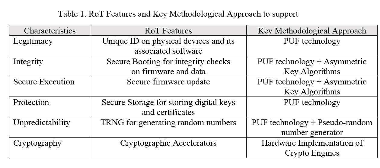
Conventionally the secret keys such as the unique ID or the device unique key along with the serial ID are usually generated by an external computer program and then injected into Non-Volatile Memory (NVM) of a secure device using an Automatic Test Equipment (ATE) as shown in Figure 1(a). The secret key information is managed using a software tool like a spreadsheet for further reference demand in the productization line. The fact that the key management is on the manufacturer’s responsibility may lead to an overhead and a risk of the secret keys being leaked. If we can eliminate the external process of key generation, it would elevate to the next security level and even contribute to cut down the cost of manufacturing and assembly.
Many research papers have been published in the PUF area. Compared to the case of external random number generation as depicted in Figure 1(a), the PUF technology does not require to inject random numbers onto the chip (Figure 1(b)). The random number is internally generated and theoretically, the number does not change at any circumstance. Depending on specific PUF technology (particularly SRAM PUF), error correction logic may be required to maintain the “repeatable” random number output.
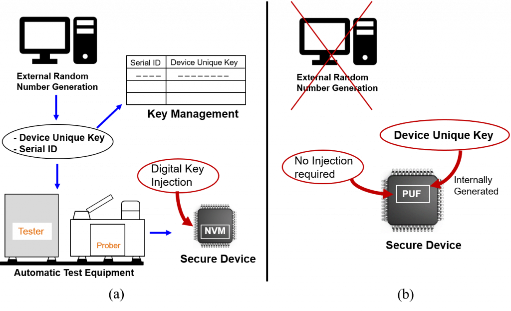
Figure 1. (a) Key injection by ATE, (b) Key generated internally in PUF technology
Why is PUF called the “fingerprint” of the silicon device?
The term “fingerprint” stands for the unchangeable “unique” pattern on human fingers. No one has the same pattern, and the pattern remains permanent. The same logic applies to the silicon device. PUF “imprints” unique patterns in silicon using an inherent process variation in wafer fabricating process, which leads to “unpredictable” value outputs (i.e. random numbers). We use the output as a unique device ID of a silicon chip, where the ID stays at the value permanently.
Since the random number is internally generated in silicon die, there is no risk of keys being exposed during wafer manufacturing and assembly process. We will go over several PUF technologies in the following section.
PUFs in general
SRAM PUF:
A SRAM cell in a standard CMOS process consists of 6 transistors including cross-coupled inverters and two bitline transistors [2] (Figure 2(a)). When the unbiased (i.e. no bias voltage induced) SRAM cell is powered on, the start-up value of the cell can be either 1 or 0 value whose direction is determined by a slight difference in threshold voltage of the cross-coupled inverters. The determining direction is unpredictable i.e. random, and the value is supposed to be repeatable every time the cell is booted up.
In reality, however, since the threshold voltage is dependent on process, voltage, and temperature (PVT) variation and device aging effect, extra helper data and error correction code (ECC) logic are additionally required to extract “stable” and a unique random number.
OTPM PUF:
The One Time Programmable Memory (OTPM) based PUF utilizes the fact that the gate oxide of a MOSFET is ruptured when a high voltage is applied on two MOSFET transistors (say left and right device) in series connection. Either the left or right one is broken down, but not both ([3], Figure 2(b)). The technology takes advantage of the randomness of oxide dopant concentration in silicon manufacturing process.
The underlying assumption of the OTPM PUF technology is that two series MOSFET devices should be in an identical matching state in the geometrical aspect. Otherwise, the claimed randomness of rupturing direction may be ended up with being biased. Device matching in advanced tech nodes is one of the challenging tasks, especially in FinFET tech nodes.
Since the technology requires high voltage input to induce the gate oxide ruptures on MOSFET devices, it could be additional overheads in design stage such as preparing high voltage pad, considering extra power line routing, and adding extra circuitry like charge pump. Adding extra testing phase in mass production stage is yet another overhead in chip yield and cost perspective.

Figure 2. Typical PUF technologies
Via PUF:
Both SRAM PUF and OTPM PUF previously stated are based on an inherent mismatch of transistor characteristics such as threshold voltage mismatch or dopant concentration mismatch in the gate oxide. Dealing with active device characteristics of a transistor is tricky since the characteristics could be altered in noisy environment, e.g. PVT variation, or aging effect of the active device, leading to reliability issues on PUF outputs.
The Via PUF technology is based on “Via” or “Contact” formation during the standard CMOS fabrication process. Note that “Via” or “Contact” is not an active device of a transistor, but a metal-like passive component used for wiring in CMOS process, which is a lot less sensitive in PVT variation than active device as shown in Figure 3.
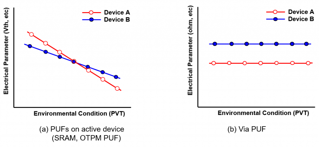
Figure 3. Variation trends of electrical characteristics such as Vth or Conductance with PVT variation in each PUF case
Via PUF Manufacturing
The technology is the outcome of the reverse thinking process. The semiconductor device fabrication process requires the device sizes to meet specific design rules to form IC devices properly in silicon. However, what if the fabrication process does not meet the design rule? Our research shows there is a middle zone in size (say PUF zone) where Via or Contact formation is at 50% of probability when the Via or Contact hole size is drawn smaller than regular design rule size. The PUF zone (XM in Figure 4(a)) exists somewhere between XL and Xs, where XL denotes the regular design rule size (i.e. 100% Via or Contact is formed) and Xs denotes a certain size that Via or Contact is not formed at all. The cross-sectional microscopic silicon image of VIA PUF is shown in Figure 4(b), where Contact hole “open” and “short” cases are clearly visible. The Contact “open” does not make the connection to the silicon substrate, while Contact “short” makes an electrical connection to the substrate.
It turns out if we pick the right PUF zone, the Via or Contact may or may not be formed during the silicon manufacturing process leading to the unpredictable or stochastic formation of Via or Contact, i.e. 50% chance of making a connection and hence, 50% chance of making no connection. After manufacturing is completed, we sort out any “barely” made holes, which are weak in reliability perspective, by measuring the resistance of Via or Contact. For example, at one technology node, the resistance over 1MΩ is identified as “open” and the one less than 50KΩ is identified as “short”, while anything between the two is sorted out. Note that the cut off value is different at each technology node. Once the connection is classified as “short” or open”, thanks to the metallic property, it stays there permanently regardless of PVT variation, which means 0% of bit error rate (BER). This is an important characteristic of Via PUF proving the robustness of the technology.
Figure 4. PUF zone at 50% probability of Via or Contact formation (sourced from [1])
Randomness
Achieving complete randomness is crucial for PUF, where ideal randomness is represented by Hamming Weight of 0.5 or 50%. The occurrence of Logic_0 and Logic_1 bits in PUF output needs to be at or close to 50% probability. Via or Contact formation alone does not satisfy the requirement. We use two-step XOR stages on “raw” PUF outputs to achieve the required randomness. For example, we fabricated 405 test chips where we designed 16 different hole sizes, 7680 bits per each hole size, a total of 122,800 bits of raw PUF outputs. The first XOR stage shrinks them to 7,680 bits, which go through the second XOR stage generating 640 bits as the final output where 0.4972 of Hamming Weight is achieved (Figure 5 (b)). The Via PUF chips went through the National Institute of Standard and Technology (NIST) SP 800-22 and SP 800-90B randomness tests and all of them passed as shown in Figure 5 (c).
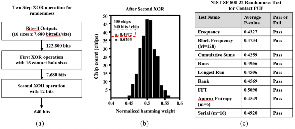
Figure 5. Two-step XOR operations for PUF randomness (sourced from [1])
Uniqueness is also an important property of PUF since it would guarantee that one chip ID is always different from other chip ID’s. The PUF chip is used for traceability of IoT devices, for example, the uniqueness of device ID is essential to trace the device along the supply chain. Uniqueness is usually defined by inter-chip Hamming Distance (HD) which can be measured by the number of different bits in two PUF outputs. If the outputs of all PUF chips are the same, the HD would be 0 which means no uniqueness. Ideally, the HD number should be 0.5 or 50% to represent the perfect uniqueness. When we calculated the HD value from the 405 Via PUF chips, we obtained 49.99% of uniqueness, which is closed to the ideal value of 50%.
Thanks to the uniqueness and the self-generation characteristic of the Via PUF technology, we use the term “InbornID” which stands for on-chip unique “inborn” ID of a silicon chip.
Reliability
The reliability of PUF means that the output is stable and unchangeable even under extreme environmental conditions. As mentioned earlier, unlike other PUFs, the Via PUF is not based on an active transistor device but is a metallic wiring material, e.g. “tungsten” or “cobalt”, whose electrical and physical characteristics do not change even under stressed PVT variations. The robustness of the technology has been verified by following the JEDEC standards in temperature, supply voltage, humidity, and pressure fluctuations for testing, resulting in none of the bitcells were flipped or changed in all 405 test chips. More details regarding the test are available in [1]. The Via PUF technology also passed the Automatic Electronics Council (ACE) Q-100 Grade 3 test for automotive applications.
Obscurity
One of the great advantages of using the Via PUF technology is “obscurity” in implementation. The Via or Contact holes are implemented scattered all around the chip. There is no need to form array blocks like the building blocks of an SRAM PUF or OTPM PUF. It is difficult to distinguish between PUF vias and regular logic vias, making IC reverse engineering practically impossible.
Standard Manufacturing
The Via PUF technology uses standard cell structures from standard digital library which runs with regular core voltage. There is no high voltage, and so no special circuitry like charge pump. There is no extra mask layer required in manufacturing stage.
Feature Summary of Via PUF
- The technology is based on the randomness of “Via” or “Contact” formation by breaking design rules in the standard CMOS fabrication process.
- Resulting in robust “open” or “short” outputs turning into unique random numbers
- Provides on-chip unique “InbornID”. No injection is necessary.
- No Error Correction Code (ECC) is necessary.
- The test results show Randomness (Hamming Weight 0.4972), Uniqueness (Hamming Distance 49.99%), and Reliability (JEDEC passed/ACE Q-100 Grade 3 passed).
- The Via or Contact holes are randomly scattered in implementation, making IC reverse engineering practically impossible.
- The technology does not introduce any special mask layer in the manufacturing process since the PUF cells are designed out of standard Via or Contact cells in digital library. No high voltage is required.
- Via PUF is a totally unique InbornID or digital key of Root of Trust similar with the fingerprint on human body.
System on Chip embedded with Via PUF
The Via PUF technology is currently in mass production embedded in several System on Chip (SoC) products. The block diagram is shown in Figure 6. The SoC is embedded with the Via PUF, the True Random Number Generator (TRNG) and the Cryptographic Accelerators such as ECC, AES and SHA256. The secure SoC supports symmetric key generation algorithms such as AES and asymmetric key generation algorithms such as ECC, ECDSA, and ECDH.
The Via PUF is part of the Secure Enclave providing Unique ID and secure storage function for storing sensitive private data. The secure SoC equipped with the key generation algorithms provides various secure functionalities such as secure authentication, firmware protection, integrity checking, anti-counterfeiting, Public Key Infrastructure (PKI), etc.
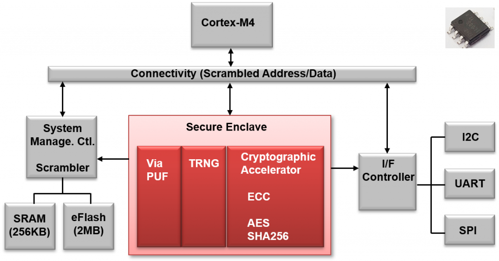
Figure 6. Block Diagram of System on Chip embedded with Via PUF
Security Functions of Hardware Root of Trust
So, what can we expect from the hardware Root of Trust based on Via PUF technology?
-The concerns on conventional PUF are relieved. The active transistor based PUF technologies have concerns on the reliability that the PUF outputs are not stable under environmental PVT variations. They try to resolve the issue by adding the Helper logic and Error Correction Code (ECC) logic blocks. The Via PUF technology does not have the reliability issue thanks to the metallic property of Contact or Via. No ECC is necessary.
-No digital key injection is necessary since the unique and random key is self-generated inside the chip. The key is a fingerprint of the specific chip.
-Key management stores secrete digital keys encrypted with unique PUF key inside the Hardware Root of Trust. The PUF key is not stored inside the chip, nor does it leave the chip. The key is rather generated every time it is demanded.
-On-Chip Unique InbornID and Traceability in trusted supply chain powered by the Via PUF technology ensure that chip production be traceable starting from manufacturing stage to all the way down to end customers in the supply chain.
-Integrity Checking and Authentication supported by Hardware Root of Trust validate the codes being executed as well as data in the secure chip.
-Secure Storage function provides a memory space for storing secrete data such as private keys using encryption and authentication with a device unique key (DUK).
-Firmware Protection by Secure Boot and Secure Update guarantees that running software is not compromised after performing authentication and decryption on the software.
-Secure Communication channel is established by completing an authentication and key exchange protocol such as Transport Layer Security (TLS). Once the secure channel is set, an ephemeral session key is shared and used for encryption and decryption. The keys are generated inside the Hardware Root of Trust.
Real Life Applications in Business
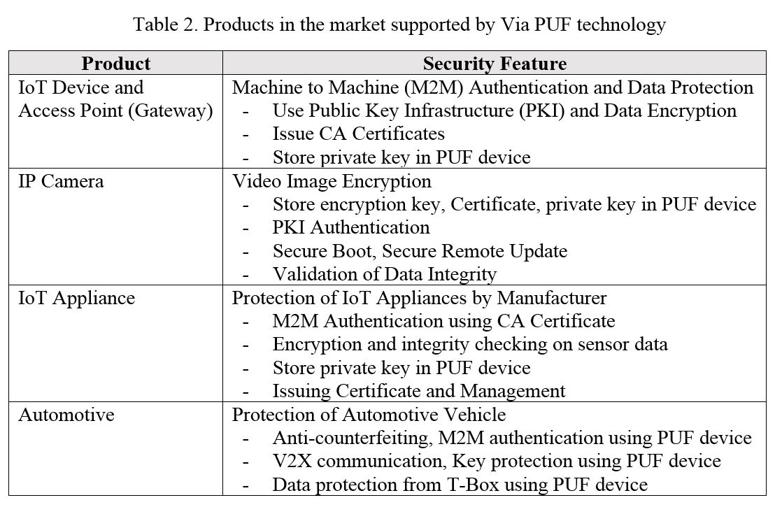
The Via PUF based RoT Chips are currently in the markets of telecommunications, appliances, and IoT devices. The products are in the forms of Wifi modules, Doorbell Ring, Smart Door Locks, IP Cameras, and IR Hubs where the functionalities such as secure boot, secure firmware copy protection, secure firmware update and secure data integrity are supported. Table 2 shows the categories of products powered by the Via PUF Technology currently in the market.
Conclusion
Unlike well-known existing PUF technology, the Via PUF technology relieves the reliability concerns thanks to the metallic property of Contact or Via, and opens doors to new business opportunity in variety of security areas including IoT devices, Trusted Supply Chain, Access Point Security, IP camera, Automotive, etc. The Via PUF is a unique InbornID or self-generated digital key in Hardware Root of Trust module which is a golden anchor that can be trusted in any circumstances.
References
[1] D. J. Jeon, et al., “A Physical Unclonable Function with Bit Error Rate < 2.3×10⁻⁸ based on Contact Formation Probability without Error Correction Code,” IEEE J. Solid-State Circuits, vol. 55, No. 3, pp. 805-816, March 2020.
[2] J. Guajardo, S. S. Kumar, G. J. Schrijen, and P. Tuyls, “FPGA intrinsic PUFs and their use for IP protection,” in Proc. Int. Workshop Cryptograph. Hardw. Embedded Syst., pp. 63-80, Sep. 2007.
[3] S. Sadana, et al., “A Highly Reliable and Unbiased PUF Based on Differential OTP Memory,” IEEE Electron Device Letters, Vol. 39, Issue 8, pp. 1159-1162, August 2018.
___________________________
About Teddy Kyung Lee | ktlee@ictk.com | www.ictk.com
Teddy Kyung Lee is an IoT security professional working on bringing security features to network components such as Serial to Ethernet, LoRa network, Smart IoT sensors, Industrial IoT, and FIDO applications. He is recently interested in Hardware Root of Trust solution using Physical Unclonable Function (PUF) technology extended from his career background in hardware SoC design.
Teddy received Ph.D. and M.S. degrees in Electrical Engineering from the University of Texas at Austin, and B.S. degree in Electronics Engineering from Seoul National University, Seoul, South Korea. He worked at IBM Research Lab, Austin, TX, and Sun Microsystems, Sunnyvale, CA, as a circuit designer in microprocessor designs. Thereafter he worked at Juniper Networks, Sunnyvale, CA, and then Altera Corporation, San Jose, CA as a methodology leader. Scouted as an overseas brain by Korean government, he worked in IoT security and FIDO applications.