In this interview, ATREG, Founder, President, and CEO Stephen Rothrock provides an overview of the global semiconductor manufacturing asset market as well as advice for global chip makers looking to divest or purchase wafer fabs in unstable global economic conditions plagued by geopolitical tensions.
Please tell us a little bit about your professional background. How did you end up in the semiconductor industry?
A little by chance really! I started in commercial real estate brokerage working as a Director for Savills International in London, UK for close to eight years. In 1997, I came back to Seattle, WA to work for Colliers International where I established the company’s Global Corporate Services initiative and headed the U.S. division working with many multinationals dealing with their portfolio of real estate assets. In the late 90s, Japan was heavily divesting from U.S. semiconductor manufacturing assets due to falling memory prices and the high exchange rate of the Yen against the U.S. Dollar. As a result, several Japanese companies approached us asking if we could help them divest some of their wafer fabs located in the Pacific Northwest. That’s how we ended up selling two 200mm fabs, including Matsushita Puyallup, WA, and Fujitsu Gresham, OR, to Microchip. Then we sold one for Sony down in Eugene, OR and NEC invited us to sell their 200mm facility in Scotland. I have always been immensely grateful to the Japanese for the trust they put in us in those early days. ATREG would not be where it is today without them.
Why did you decide to create ATREG back in 2000? What problems does your company solve for global chip makers?
After closing these fab transactions for Japanese companies while working at Colliers International, I recognized a gap in the market and decided to create a special internal division named Advanced Technology Real Estate Group (ATREG), dedicated exclusively to transactions focused on infrastructure-rich semiconductor cleanroom and manufacturing assets. We realized that if we sold the facility with an operational tool line, workforce, and ongoing supply agreement, there was a market for wafer fab divestment and acquisition services to other chip makers at a time when the industry was consolidating, not just in Asia, but also in the U.S. and in Europe. The business took off. In August 2010, I spun ATREG out of Colliers International. There was a real need to help advanced technology companies with their global manufacturing strategies because they didn’t know where to start. As we continued to conduct fab transactions, we collected significant data on cleanroom assets and critical deal points. Most companies didn’t have the staff or knowledge internally to conduct these transactions in a timely manner. Trust and integrity were key to discussing these very sensitive issues given the financial and balance sheet effect. Over time, ATREG has built trusted relationships with many of the high-level C-suite executives in the semiconductor industry to facilitate these transactions. Our key objective is to work hand in hand with sellers and buyers alike to find the right asset strategy while simultaneously retaining as much human capital as possible when fabs change hands.
What lessons could we draw from a quick history of global wafer fab transactions?
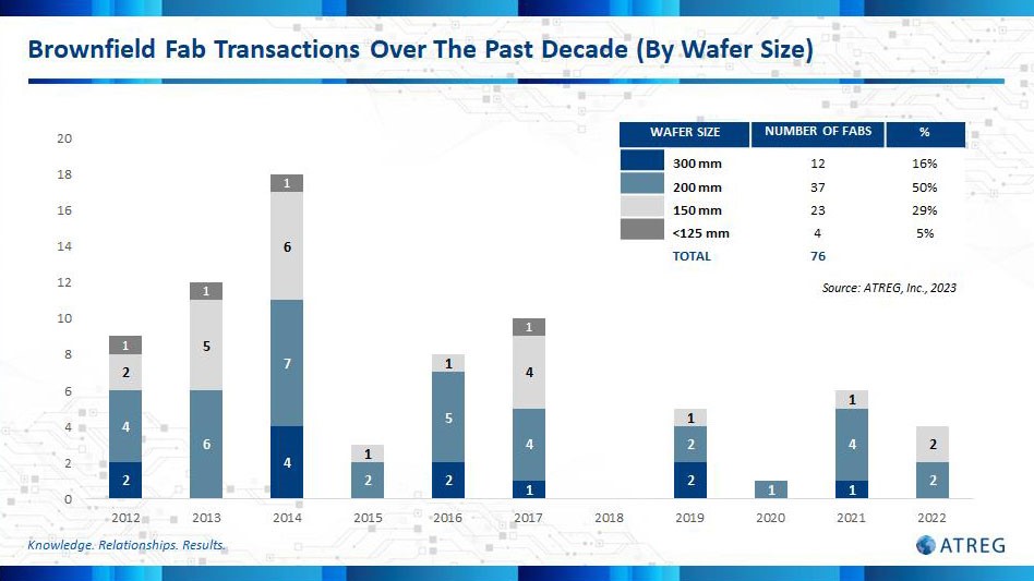
The surge in fab transactions after the 2008-2010 recession was followed by a significant tapering-off from 2015 to 2020 with an average of 4.5 fabs sold per year. Industry consolidation was a factor in this low number due to 250 M&A deals over a 12-year period valued at over $500 billion, nearly three times the amount of the previous 12 years. It’s been a buyers’ market over the last five years, but that is changing in the current environment. Some 38 200m fabs have sold and in 2021, that trend continued with five, four of which are 200mm. There was a comeback in 2021 among tight supply constraints, risks associated with geopolitical tensions, companies put on allocation, and steady rises in pricing. Now we are back in a market downturn, with a global chip shortage exacerbated by the aftermath of a global pandemic and wafer fabs are now needed more than ever before.
Then this begs the question: How many fabs are there currently worldwide?
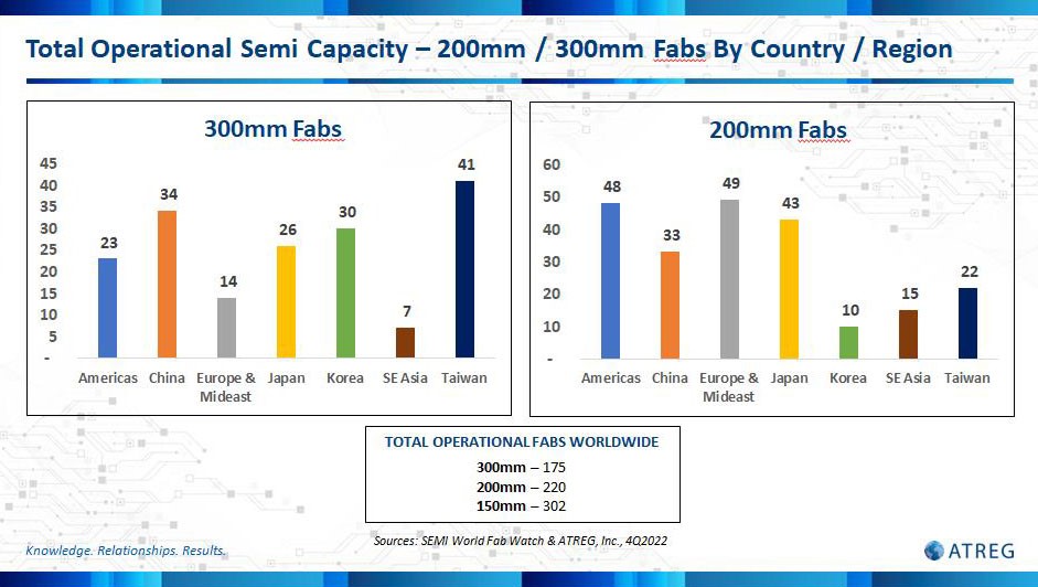
Let’s look at a fab breakdown by country / region. There are currently only 175 300mm fabs total in the world which is not a huge number. Korea has 30 fabs, but significantly fewer campuses overall as they are concentrated in Samsung megasites which have much larger capacity than U.S. ones. Many existing facilities these past two years have been running at 100%+ capacity and tools are constrained. Many 200mm users are buying 300mm tools and calibrating them back to 90nm, .13, and .18 nodes. The large majority of new fab projects between 2019 and 2022 were 300mm. The U.S. and Europe have the most 200mm fabs, but APAC, Taiwan, and China hold 50% more 300mm fabs than the U.S. and Europe combined (111 vs. 55).
Do you believe that the recently passed U.S. CHIPS Act will help bring silicon chip manufacturing back to U.S. shores? Will that funding be enough for U.S. semiconductor manufacturing to compete with Asia?
This is one reason why the U.S. has deemed it critical to bring semiconductor manufacturing back to U.S. shores. U.S. leadership on the world stage depends on it. China has been subsidizing their domestic chip making by the boatload for over 10 years. It will be hard enough for the U.S. to catch up, even harder to leap ahead. This initial public funding of $52 billion is a great start, but while this package will help us keep pace with incentive programs around the world for now, it is nowhere near enough over the long term. The U.S. administration will need to do more and soon.
The first call for CHIPS Act application funding opened up at the end of February for projects to construct, expand, or modernize commercial facilities for the production of leading-edge, current-generation, and mature-node semiconductors, including both front-end wafer production and back-end packaging fabs. This is an encouraging first step for many universities, start-ups, and global companies to engage in solving our chip shortage. I think we can all agree that we want these public funds to be spent wisely and we will get more insight into the process over time as applications get reviewed by the U.S. Administration.
In the end, who will be the big winners of the CHIPS Act funding?
The big winners of the CHIPS Act funding will be as follows:
Companies that can execute a greenfield site selection process quickly – A great American semiconductor manufacturing success story is silicon carbide semiconductor producer Wolfspeed. The U.S. company was one of the first to get on the incentives bandwagon in Mohawk Valley by selecting the shovel-ready Marcy Nanocenter site near Utica, NY. The world’s first, largest, and only 200mm silicon carbide fabrication facility was inaugurated and started production in April 2022.
Aerial rendering of the new Wolfspeed Mohawk Valley fabrication – the world’s largest Silicon Carbide fabrication in Marcy, New York.
Companies bringing capital to the table – The U.S. Administration does not plan to fund entire projects, but rather offer grants of between 5% to 15% of a company’s capital expenditures for a project, with funding not expected to exceed 35% of the cost. Companies can also apply for a tax credit reimbursing them for 25% of project construction. So far, more than $200 billion in private investments for U.S. semiconductor manufacturing have been committed since the CHIPS Act was signed into law last year.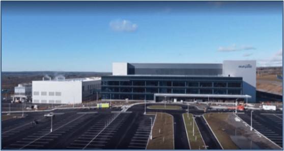
Companies committed to their community – Those who will be creating hundreds of regional skilled jobs in a very tight labor market and will implement programs that will attract women into the semiconductor workforce, such as affordable, high-quality childcare, as well as training programs for the local school, college, and university students.
What is the role of semiconductor clusters in all of this?
Semiconductor clusters are crucial to our success. As part of the CHIPS Act, we anticipate that at least two U.S. manufacturing clusters will be built to produce the most advanced types of logic chips, as well as facilities for other kinds of chips, and complex supply networks to support them. In light of where most greenfield builds are already happening, it is everyone’s educated guess as to which locations will be the lucky ones. But for our clusters to be able to support the complex needs of newly built greenfield fabs, endemic fab ecosystem issues first need to be addressed. For these funds to be fully optimized, the U.S. government needs to find ways to curb ramping inflation impacting the cost of materials, solve supply chain issues, support regional skilled job creation, and reform permits, certifications, and entitlements that are slowing down U.S. fab construction.
What is the current state of legacy / brownfield wafer fabs in the U.S.? What strategic features or factors make brownfield fabs valuable?
There has been a global shortage of operational brownfield fabs for years now and ATREG expects this to continue through to at least mid-2025. Brownfield fab demand is at an all-time high, especially 200mm fabs and tools, driven by fear of allocation and the desire for internal manufacturing control. Quite a few of these have changed hands in the past couple of years, including recently Onsemi’s South Portland, ME, and Pocatello, ID facilities, with new ones to be announced in the coming months.
Brownfield fabs are valuable because they are already operational – they offer accelerated time-to-market, the potential to maintain positive cash flow (with long-term supply agreements), already installed tool lines, equipment, and infrastructure, available intellectual property, and know-how, as well as an operational highly-skilled workforce. A great example of the importance of the latter in light of the rampant skilled labor shortage we are experiencing is Texas Instruments’ acquisition of Micron’s 300mm Lehi, UT fab that included 1,215 employees, a major asset for the company.
How will new greenfield fabs coming online over the coming months affect U.S. semiconductor capacity?
According to the Semiconductor Industry Association, over $210 billion in private investments have already been announced across 20 states to increase domestic manufacturing capacity with greenfield builds on U.S. soil alone, a large part from powerful Asian semiconductor players such as Samsung in TX and TSMC in AZ who have a significant lead over their U.S. counterparts. U.S. power players such as Intel, IBM, Micron, and Texas Instruments have embarked on aggressive fab expansions to be able to claim some of that support, respectively in OH, NY, TX, and UT.
U.S. greenfield fab projects include Micron ($15B in ID, $20B in NY), Intel ($21B in AZ, $22B in OH), TSMC ($40B in AZ), Samsung ($18.1B in TX), Texas Instruments ($13B in TX, $11B in UT), SkyWater ($1.4B in IN), Wolfspeed ($5B in NC), GlobalFoundries ($4B in NY), and GlobalWafers ($5B in TX). No need to mention that there will be fierce competition for engineering resources, tools, and most of all skilled labor, not just for fab operations, but also tradesmen such as electricians or plumbers for fab construction.
What are the strategic benefits of selling and buying fabs for chip makers?
There are a number of benefits on both sides of the equation. On the sell side, they include fabless or fab-lite strategic initiatives, gross margin pressure, and underutilization whose root cause is often demand based. In addition, we have products coming to their end of life, CapEx requirements to continue advancing technology capabilities (there are infrastructure limitations for a site to move from 200mm to 300mm), and consolidation into other fabs, often for cleanroom shell sales. Examples include Onsemi which needed to consolidate its U.S. fab portfolio to come out of low-margin businesses. Buying the East Fishkill 300mm fab gave the company 2.5 times more capacity. In Asia, Allegro Microsystems sold a cleanroom in Thailand to consolidate all of its production to its site in the Philippines where it had extra space.
On the buy side, what makes fabs valuable is different from the driving force behind a purchase. Core reasons include geo-political de-risking, allocation, and manufacturing control, scaling geometry requirements, and product demand. Examples include Diodes and their desire for increased internal manufacturing control, Texas Instruments and scaling geometry requirements, or VIS and increased demand for products requiring additional capacity.
What is the best advice you would give U.S. chip makers to ensure successful manufacturing in 2023 and beyond?
If there was one piece of advice I could give U.S. semiconductor manufacturers to ensure capacity and supply chain resilience, it would be that they leave no stone unturned by looking at all semiconductor manufacturing options at their disposal. Greenfield fabs with support from CHIPS Act funding is one, but it will take years before these new facilities yield as long as permits, certifications, and entitlements are not reformed in the U.S. Plus the competition for those public funds will be fierce. The other alternative to consider is brownfield. These facilities are obviously few and far between at any one time, but as chip makers who wish to go fab-light or fabless transition their production out to foundries, some operational fab assets will become available on the market all over the world and there might just be one out there that’s right for you. E.g. companies in compound semi, GaN, GaAs, SiC, and MEMS want fabs and greenfield is not necessarily the answer for them because they are too long to yield.
Can you give us your vision for the global semiconductor landscape for the next few years?
I think it is fair to say that the U.S. CHIPS Act funding package is a great start, but it will be nowhere near sufficient in the long term for the U.S. to regain its semiconductor manufacturing leadership on the global stage. We will need more government incentive packages somewhere down the line to sustain that effort. The solution is to balance short-term investments that shore up capacity with spending aimed at mastering cutting-edge manufacturing, as well as longer-horizon R&D of next-generation technologies.
We will need additional action from the U.S. Administration on other fronts as well to help solve the many challenges exacerbated by the Covid pandemic – geopolitical tensions, skilled talent shortage, rising capital and operational expenditures, shorter product, and demand cycles, longer lead times for components (x2) and equipment (x2.5), supply chain challenges, fab construction costs (2x), and sustainability issues to name just a few. Although U.S. fab construction companies are doing what they can to renovate, reengineer, and bring down the time we take to build fabs, the U.S. really needs to take a page out of Taiwan’s book by passing urgent reform to speed up greenfield fab construction. Getting the necessary permits, certifications, and entitlements are slowing us down greatly. If Taiwan can build significant fabs in less than 24 months, why couldn’t we?
About Stephen M. Rothrock
 Stephen founded ATREG in 2000 to help global advanced technology companies divest and acquire infrastructure-rich manufacturing assets, including wafer fabs (front- and back-end) as well as MEMS, solar, display, and R&D facilities. Over the last 24 years, his firm has completed over 100 transactions, representing over 40% of all global operational wafer fab sales in the semiconductor industry for operational, warm, and cold shells. Recent global acquisitions and dispositions have involved Allegro Microsystems, Elmos, Fujitsu, GlobalFoundries, IBM, imec, Infineon, JDI, Matsushita (Panasonic), Micron, NXP, Onsemi, Sony, Qualcomm, Renesas, Robert Bosch, Texas Instruments, and VIS to name just a few.
Prior to founding ATREG, Stephen established Colliers International’s Global Corporate Services initiative and headed the company’s U.S. division based in Seattle, Wash. Before that, he worked as Director for Savills International commercial real estate brokerage in London, UK, also serving on the UK-listed property company’s international board. He also spent four years near Paris, France working for an international NGO. Stephen holds an MA degree in Political Theology from the University of Hull, UK and a BA degree in Business Commerce from the University of Washington in Seattle, USA.