Written by Paul Cuddyer | Director of Sales | Technetics | paul.cuddyer@technetics.com
Abstract
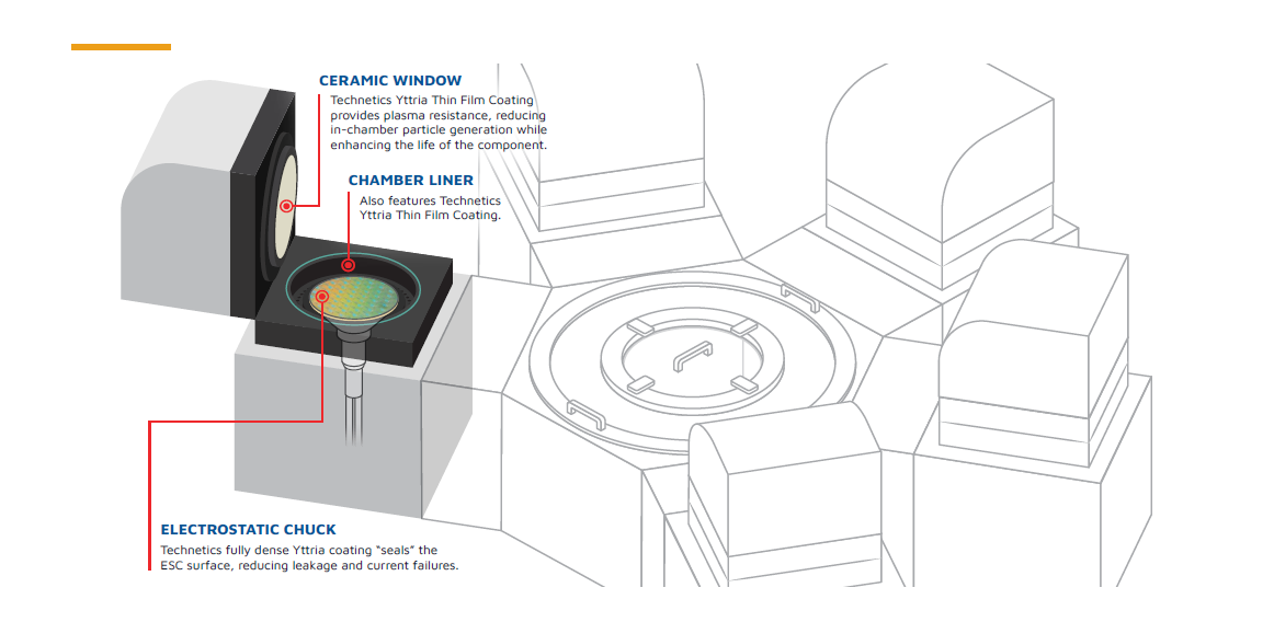
Technetics Group’s novel thin film coatings provide a fully dense, non-porous, etch resistant uniform coating that can be used to extend the life of process chamber components, reduce particle levels within a chamber, or “cap and seal” Electrostatic Chucks to provide leakage current control. With full chemical cleaning and analytical test capabilities we can provide solutions for your brand-new process chamber components, or refurbish existing components, bringing them back to a brand-new state all under one roof.
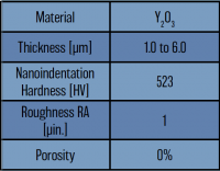
 Results from Coated Samples
Coatings were deposited on various materials including high purity alumina, quartz, sapphire and silicon to determine the film’s quality and performance on each material.
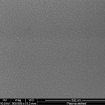
A sample was inspected at an independent analytical service company using scanning electron microscopy.
Thin film Yttria coating is applied to the substrate using a proprietary low temperature deposition process in a high vacuum chamber environment.
Film property modification capabilities include adhesion control, morphology, density, stress level, crystallinity and chemical composition.
Cross section of the Yttria deposited film.
Film thickness was measured at 6.07um and demonstrated excellent uniformity.
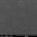
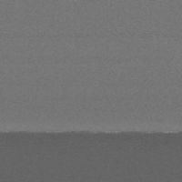
Figures: cross section of deposited film (left) | high magnification of the deposited film demonstrates zero voids (right)
Thin film Yttria coating is applied to the substrate using a proprietary low temperature deposition process in a high vacuum chamber environment.
Film property modification capabilities include adhesion control, morphology, density, stress level, crystallinity and chemical composition.
Applications
The deposition is a highly etch-resistant thin
film coating that reduces particle generation
and increases chamber component lifetimes.
Figures: pre-etch (left) | post-etch (right)
Analytical work performed at an independent analytical service company. A final surface inspection was performed to determine surface roughness pre-and post-etch.
Initial etch testing
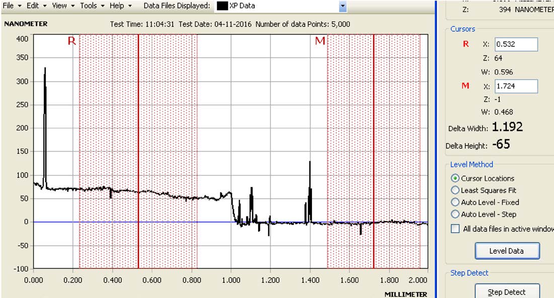
Etch testing was performed using an RIE system to determine initial etch resistance capability. Using a profilometer, an etch depth of about 60 nm was determined after a 30 min process in CF4 + O2 chemistry.
Test 2 was processed in a semiconductor facility
With CF4 chemistry, the sample ran for a total of 8.7 hours and the etch rate was determined to be approximately 750 Angstroms.
Results (Quartz Sample)
Etch depth measurement after RIE process (30 min) uniformity.
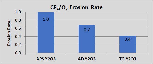
APS – Atmospheric Plasma Spray
AD – Aerosol Deposition
TG – Technetics Group
The samples demonstrate superior etch resistance to aerosol deposition and other thin-film coatings. Additionally, the surface morphology changes are constant with low- etch and high-etch resistance, and the cross-sectional images indicate no porosity, providing a very dense film, which is consistent with the low-etch rate observed.