Lucio Lanza
Managing Director
Lanza techVentures
David Kelf
Chief Executive Officer
Breker Verification Systems
Semiconductor verification over the last 30 years or so evolved in three major cycles, the most recent occurring right now, combined with multiple smaller developments. Although it has been suggested that verification effort has increased as a squared law to design size, this hypothesis is simplistic at best. A thorough understanding of verification trends and their drivers may assist semiconductor development teams to improve or, at least, predict their schedules more effectively.
 Driven by sweeping changes in integrated circuit design, verification remains the leading development bottleneck, both in terms of pure resource deployment and a lack of schedule predictability. Verification occupies more than 70% of the development cycle, and it’s getting worse. Furthermore, the slowdown in Moore’s Law, leading to a reduction in silicon acceleration, has driven a corresponding increase in design complexity as semiconductor companies attempt to maintain differentiation. This, in turn, has an exponential effect on the verification requirement.
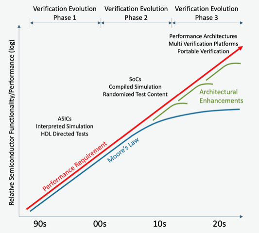
A further examination of verification methodologies and approaches demonstrates a twin cycle, symbiotic relationship between execution platforms and test content approaches within this broad, three-phase evolution as shown in figure 1. With platform driving content driving platform in an, arguably, tail-wagging-the-dog series of cycles, the modern verification approach tracks:
Verification evolution 1: ASICs, Interpreted Simulation and HDL tests
Back 30 or so years ago, the industry saw the advent of Hardware Description Languages (HDLs) driving Application Specific Integrated Circuits (ASICs) where multiple ASICs would be integrated on a circuit board and driven by an independent processor. Gate-level ASIC designs gave way to Register Transfer Level (RTL) descriptions and the use of synthesis. HDL interpreted simulation became the execution platform of choice and the initial test content in the form of directed tests, coded as streams of 1s and 0s quickly was replaced by programmed HDL test content. System-level validation was reserved for the final circuit card containing all devices and software, which was then bombarded with real world data in the form of test workloads. Although the world has moved on from this methodology, many hangovers exist that limit overall progress.
Verification evolution 2: SoCs, Compiled Simulation and Randomized Test Content
As silicon capacity dramatically increased, a line was crossed where it was possible to place the processor IP on the chip together with all required custom blocks that had been ASIC-based, resulting in the first system on chips (SoCs). This drove a massive need for increased verification performance delivered in the form of compiled-code simulation as opposed to the previous interpreted tools. With the increase in block complexity now unconstrained by ASIC boundaries, and the corresponding 10X or more simulation performance boost, engineering teams encountered the next inevitable roadblock; the ability to compose test content in acceptable timeframes that could dig deep into operational corner cases to drive required test coverage. Constrained Random Test Generation, now embodied in SystemVerilog and UVM, was a breakthrough that revolutionized test content composition and disrupted the entire process, creating a new breed of verification engineer and enabling a step function in overall productivity.
Verification evolution 3: Performance Architectures, Multi-Execution Platforms, Portable Verification
Once again, a fundamental change in design approach is driving current verification evolution. Over the last few years, the expense of fabrication technology advancements has led to a decline in Moore’s Law acceleration. Semiconductor technology enhancements provided a relatively easy way for semiconductor companies to provide continuous improvements in design specifications.
With Moore’s Law tapering off, engineering teams are exploring new ways to achieve this same goal, inevitably leading to increased design complexity and verification requirements. Powerful revolutionary processor architectures, co-processing blocks providing hardware acceleration, the RISC-V Open Instruction Set Architecture (ISA) which allows custom instructions to be tightly integrated into processing cores, improvements in memory architectures and communication protocols, for example, have driven verification complexity.
Indeed, the addition of incremental processors within systems to provide raw and application-specific processing power is important. Multi-core processing was used to amplify raw processing power, pushing the acceleration problem to the software running on the combined system and creating a new SoC verification issue. This was augmented by co-processing used to accelerate particular functions, often mathematical data processing in nature, which again required specialized scenario testing. Today advanced processors such as AI/ML arrays that leverage software and hardware together to provide basic functionality must be tested with a hardware/software verification approach.
The tail of the Moore’s Law S curve is slowing and, in turn, driving several new, exponential opportunity S curves. This has been further compounded by new “Integrity Verification” requirements such as safety, security, SoC infrastructure, early firmware (or “software first”) test all falling to verification teams. Applications such as medical, automotive and others are particularly susceptible to these integrity issues.
Then there’s the open-source silicon movement that offers the promise of chip design anywhere/anytime and this is changing the nature of design IP delivery and its integration. Instead of large semiconductor companies obtaining IP from various sources and taking responsibility for the overall SoC functional integrity, we have the specter of smaller companies integrating their proprietary IP onto complete SoCs provided by larger providers. This highly beneficial evolution has one drawback: Which company takes responsibility for device quality and, therefore, who provides and executes the test content that must encompass the IP and the surrounding SoC? A modular approach is required.
Phase 3 Verification Methodology Trends
These changes have led to verification evolution on multiple axis. Design complexity naturally leads to verification complexity and these exponential opportunity curves drive entirely new needs in test methodology. The Verification Requirement expanding from pure functional test to full integrity assurance also drives new methodology thinking.
The third axis, the execution platform explosion providing multiple options for exercising verification with their own corresponding test content format and debug, has both positive and negative ramifications. While providing options that trade off verification performance for flexibility throughout the development flow is very effective, the use model of each platform is compartmentalized leading to wasted effort. Once again, an evolution in execution platforms is driving a corresponding change in test content.
Verification portability across these platforms is critical from the point of view of not repeating resource-intensive test content composition. Nevertheless, the problem goes much further. When test content developed for one platform is used on another, inefficiencies in execution, engineering interaction, test reuse and results analysis are evident. The evolution of Phase 3 test content composition is a bottom-up process that leads to cracks that widen as design requirements become more stringent even in individual phases –– for example, the inability to scale UVM sequences to sub-systems or reuse them in SoC emulation.
If this is not bad enough, the Lego-like methodology of block functional verification followed by real workloads across the full SoC, the hangover from Phase 1, is breaking down. That’s a result of more functionality spread across the SoC blocks, implemented in powerful co-processors that interact with software and leverage coherent architectures with increased integrity requirements. A verification “gap” is widening where the initial SoC verification cannot be accomplished by running real workload data and requires specialized test content of its own. A perfect example is system coherency where next-generation designs make use of advanced memory and fabric architectures, creating corner-case complexity so extreme that years of emulation time would be required to uncover them. Specialized algorithms are necessary to track them down that need to be encompassed in encapsulated test scenario models.
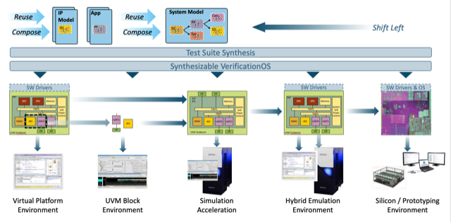
We therefore arrive at Verification Evolution Phase 3 test content composition. Test content must be created top down, not bottom up as shown in figure 2. Verification goals based on the design specification need to be set and separated from the implementation of the test content for the various individual verification phases. This evolution occurred before in semiconductors in the form of design synthesis. Test content composition requires a synthesis approach, and technologies are now emerging to provide this paradigm.
Synthesis can solve many of the issues across modern verification methodologies. It will allow test methods to scale and make full use of the verification platforms available, create a configurable reuse approach to save vast composition effort and provide the quality coverage necessary for integrity requirements. Much like the phase 2 knock on affect in engineering specializations, phase 3 will allow engineers to share high-level test content while easily maintaining their own areas of specializations by exploiting environmental layers. This will streamline overall team interaction in the new Portable Verification methodology.
About Lucio Lanza
 Lucio Lanza is the Managing Director of Lanza techVentures, an early-stage venture capital and investment firm, and the 2014 recipient of the Phil Kaufman Award for Distinguished Contributions to Electronic System Design. Earlier in his career, Dr. Lanza held executive positions at Olivetti, Intel, Daisy Systems, EDA Systems and Cadence Design Systems. While serving as head of Intel’s Microprocessor Strategic Business Segment (SBS) in the 1980s, Dr. Lanza convinced Phil Kaufman and Intel management to co-design the first controller device for the Ethernet networking standard with Digital Equipment Corporation and Xerox. Dr. Lanza joined the venture capital industry in 1990. He served as a non-executive director of Arm, the leading semiconductor IP company, and was chairman of the board of PDF Solutions, Inc., a provider of technologies to improve semiconductor manufacturing yield.
He currently sits on board of directors of several private companies and served as a member of the board of directors of Harris & Harris Group, an investor in transformative companies enabled by disruptive science. Dr. Lanza holds a doctorate in electronic engineering from Politecnico in Milan, Italy.
About David Kelf
 David Kelf holds the position of CEO of Breker Verification Systems. Prior to that, as Chief Marketing Officer, he was responsible for all aspects of Breker’s marketing activities, strategic programs and channel management. Earlier, he served as vice president of worldwide marketing solutions at formal verification provider OneSpin Solutions (now Siemens EDA). Kelf was president and CEO of Sigmatix, Inc. and the verification marketing director at Cadence Design Systems responsible for the Verilog and VHDL verification product lines. As vice president of marketing at Co-Design Automation and then Synopsys, Kelf oversaw the successful introduction and growth of the SystemVerilog language, before running marketing for Novas Software that became Springsoft and is now part of Synopsys. Kelf holds a Bachelor of Science degree in Electronic Computer Systems from the University of Salford and a Master of Science degree in Microelectronics from Brunel University, both in the U.K., and an MBA from Boston University.